H8DGi: Difference between revisions
Jump to navigation
Jump to search
No edit summary |
No edit summary |
||
| Line 35: | Line 35: | ||
== Board Layout == | == Board Layout == | ||
[[File:H8DGI Diagram.png| | [[File:H8DGI Diagram.png|600px|alt=Alt Text|thumb|Caption]] | ||
[[File:H8DGI BlockDiagram.png| | [[File:H8DGI BlockDiagram.png|600px|alt=Alt Text|thumb|Caption]] | ||
== Flashing == | == Flashing == | ||
[[File:1000001278.jpg| | [[File:1000001278.jpg|600px|alt=Alt Text|thumb|Caption]] | ||
External flashing is required. The stock BIOS chip is a 2 MiB SOIC8 located below PCIe slot 2, next to the NVRAM battery. | External flashing is required. The stock BIOS chip is a 2 MiB SOIC8 located below PCIe slot 2, next to the NVRAM battery. | ||
Revision as of 14:17, 31 August 2024
| H8DGi | |
|---|---|
 | |
| Overview | |
| Introduced | TBD |
| Manufacturer | Super Micro |
| Specifications | |
| Socket | 2x G34 |
| Northbridge | 2x AMD SR5690 |
| Southbridge | AMD SP5100 |
| Super I/O | Winbond W83527 |
| BMC | Winbond WPCM450 BMC |
| BMC Flash Location | Onboard Module |
| Memory | 16 slots (8 channels) DDR3-1600 ECC RDIMM/UDIMM, up to 512GB on coreboot |
| BIOS Flash | 2 MiB soldered |
| Form Factor | E-ATX |
| Power Inputs | 2x 8-pin EPS |
| Expansion Slots |
|
| Onboard Peripherals | |
| Graphics Adapter | Matrox G200 16MB DDR2 |
| Network Interface | 2x Intel 82576 Gigabit |
| Storage Controller | SP5100's SATA2 (3.0 Gbps) |
| USB Controller | SP5100's onboard USB 2.0 |
| Serial Interface | One SIO-provided RS232 |
| Audio Interface | None |
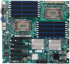
The Super Micro H8DGI is a dual-socket server/workstation motherboard with support for Socket G34 Opteron processors. Support for the H8DGI was added in coreboot-fam15.
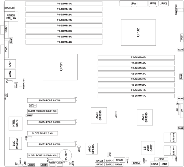
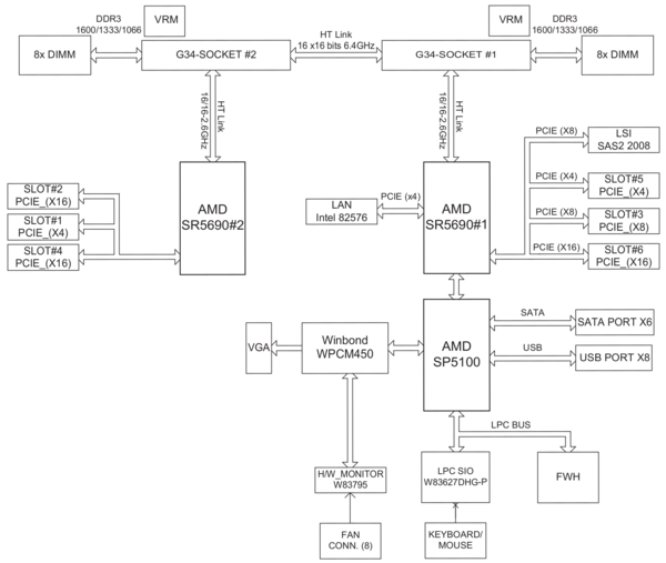
Board Layout


Flashing

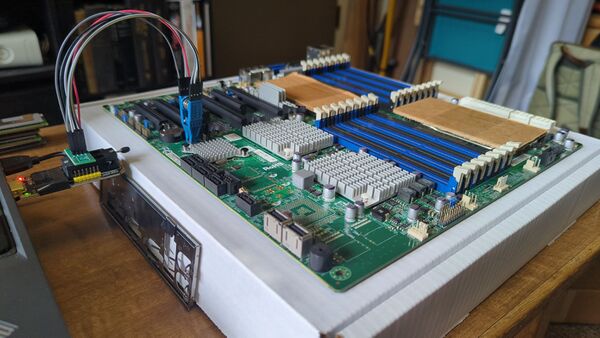
External flashing is required. The stock BIOS chip is a 2 MiB SOIC8 located below PCIe slot 2, next to the NVRAM battery.