H8SCM: Difference between revisions
No edit summary |
|||
| Line 43: | Line 43: | ||
== Board Components == | == Board Components == | ||
=== Socket C32 === | |||
{{Excerpt|Socket C32|inline=yes|bold=yes}} | |||
==== AMD Opteron 4100 Series ==== | |||
{{Excerpt|AMD Opteron 4100 Series|inline=yes|bold=yes}} | |||
==== AMD Opteron 4200 and 4300 Series ==== | |||
{{Excerpt|AMD Opteron 4200 and 4300 Series|inline=yes|bold=yes}} | |||
=== AMD SR5650 === | === AMD SR5650 === | ||
{{Excerpt|AMD SR5650|inline=yes|bold=yes}} | {{Excerpt|AMD SR5650|inline=yes|bold=yes}} | ||
Revision as of 18:15, 31 March 2025
| H8SCM | |
|---|---|
 | |
| Overview | |
| Introduced | 2010 |
| Manufacturer | SuperMicro |
| Specifications | |
| Socket | 1x C32 |
| Northbridge | AMD SR5650 |
| Southbridge | AMD SP5100 |
| Super I/O | Winbond W83527HG |
| BMC | Nuvoton WPCM450 |
| BMC Flash Location | Onboard |
| Memory | 4 slots (2 channels) DDR3-1600 ECC RDIMM/UDIMM, up to 128GB |
| BIOS Flash | 2 MiB soldered SOIC-8 (W25Q16V) |
| Form Factor | u-ATX |
| Power Inputs | 1x 8-pin EPS |
| Expansion Slots |
|
| Onboard Peripherals | |
| Graphics Adapter | Matrox G200eW |
| Network Interface | 2x Intel 82574L Gigabit |
| Storage Controller | SP5100's SATA2 (3.0 Gbps) |
| USB Controller | SP5100's onboard USB 2.0 |
| Serial Interface | One external, one internal |
| Audio Interface | None |
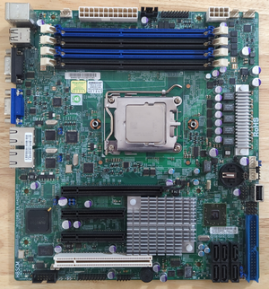
The H8SCM motherboard is highly supported by coreboot-15h.
Board Variants
H8SCM
H8SCM-F
The H8SCM-F is identical to the H8SCM, but has an onboard BMC. It is compatible with the coreboot image for the H8SCM, but it is not known whether the onboard BMC will operate. The "JPB1" motherboard jumper can be used to disable the onboard BMC, effectively turning the H8SCM-F into the H8SCM.
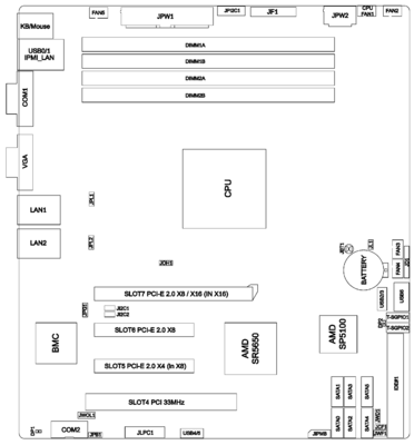
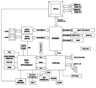
Board Diagrams
Board Components
Socket C32
Socket C32 is compatible with AMD Opteron 4000 series processors. All compatible CPUs contain a single NUMA node. CPU coolers designed for Socket F are compatible with Socket C32.
AMD Opteron 4100 Series
Processors in the AMD Opteron 4100 Series were designed with the K10 microarchitecture and are compatible with the C32 socket.
Official Source Code and Documentation
- AGESA Source Code
- AGESA Interface Specification
- BIOS and Kernel Developer's Guide
- Product Data Sheet
- Power and Thermal Data Sheet
AMD Opteron 4200 and 4300 Series
Processors in the AMD Opteron 4200 and 4300 Series were designed with the Bulldozer (4200 series) and Piledriver (4300 series) microarchitectures and are compatible with the C32 socket.
Official Source Code and Documentation
- AGESA Source Code
- AGESA Interface Specification
- BIOS and Kernel Developer's Guide
- Product Data Sheet
- Software Optimization Guide
AMD SR5650
The AMD SR5650, previously known as RD870S, is a powerful system logic designed for the server/workstation platform. The SR5650 boasts 26 PCI Express® (PCIe®) lanes, with 22 lanes dedicated to external PCIe devices and 4 for the A-Link Express II interface to AMD's Southbridges like the SP5100 (formerly SB700S). The chipset is also equipped with the latest HyperTransportTM 3 and PCIe Gen 2 technologies, delivering exceptional performance in a compact 29mm x 29mm package.[1]
Official Source Code and Documentation
- CIMx Source Code
- BIOS Developer's Guide
- IOMMU Specification
- Register Reference Guide
- Register Programming Requirements
- Product Databook
- Product Errata
AMD SP5100
The AMD SP5100 is a versatile Southbridge designed to complement AMD's server Northbridges, integrating essential I/O, communication, and other features for advanced server platforms into a single device. [2]
Official Source Code and Documentation
- CIMx Source Code
- BIOS Developer's Guide
- Register Reference Guide
- Register Programming Requirements
- Product Databook
- Product Errata
Part Numbers
- AMD 218-0660013
- AMD 218-0660024
- AMD 218-0660026
Nuvoton WPCM450
The Nuvoton WPCM450 is a combined Baseboard Management Controller and 2D/VGA-compatible Graphics Core with PCI Interface, Virtual Media, Keyboard and KVMR Module[3]. Multiple vendors shipped the WPCM450 with Linux, making it feasible to build an open source replacement for the original BMC firmware[4][5][6]. 3rd party documentation and tools have been developed by neuschaefer and are available on github. The WPCM450 appears to be related to, or based on, the Winbond W90N745.
Flashing Firmware
To switch from the stock firmware to coreboot, external flashing is required.
Flash Chip Location
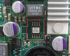
The flash chip is located above the circular CMOS battery slot.
Flash Chip Orientation
The circle marking the location of pin 1 is highlighted red in the above image. The circle is a subtle indentation on the chip that can be seen with the aid of a flashlight.
Flashing Example
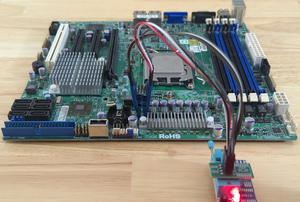
A CH341a programmer can be used to flash coreboot onto the H8SCM.
User Builds
References
- ↑ https://theretroweb.com/chips/5698
- ↑ https://theretroweb.com/chips/5699
- ↑ https://theretroweb.com/chips/10379
- ↑ https://github.com/neuschaefer/linux/tree/vendor/wpcm450-aten
- ↑ https://github.com/neuschaefer/linux/tree/vendor/wpcm450-ami
- ↑ https://github.com/neuschaefer/linux/tree/vendor/dell-idrac6-1.70
