H8QGi+-F: Difference between revisions
No edit summary |
No edit summary |
||
| Line 52: | Line 52: | ||
The H8QG7-LN4F is a H8QG7+-LN4F with a secondary northbridge and additional PCIe lanes. It is likely compatible with the coreboot image for H8QG6+-F, but this has not been tested; the secondary northbridge and associated PCIe lanes will be offline. | The H8QG7-LN4F is a H8QG7+-LN4F with a secondary northbridge and additional PCIe lanes. It is likely compatible with the coreboot image for H8QG6+-F, but this has not been tested; the secondary northbridge and associated PCIe lanes will be offline. | ||
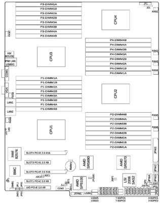
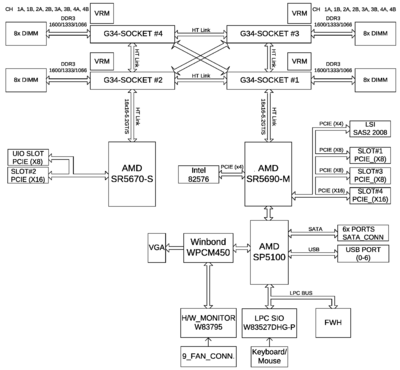
== | == Board Diagrams == | ||
[[File:H8QGi Diagram.png|frameless|400x400px]] | |||
[[File:H8QGi BlockDiagram.png|frameless|400x400px]] | |||
== Board Components == | |||
=== Socket G34 === | |||
{{Excerpt|Socket G34|inline=yes|bold=yes}} | |||
==== AMD Opteron 6100 Series ==== | |||
{{Excerpt|AMD Opteron 6100 Series|inline=yes|bold=yes}} | |||
==== AMD Opteron 6200 and 6300 Series ==== | |||
{{Excerpt|AMD Opteron 6200 and 6300 Series|inline=yes|bold=yes}} | |||
=== AMD SR5690 === | |||
{{Excerpt|AMD SR5690|inline=yes|bold=yes}} | |||
=== AMD SR5670 === | |||
{{Excerpt|AMD SR5670|inline=yes|bold=yes}} | |||
=== AMD SP5100 === | |||
{{Excerpt|AMD SP5100|inline=yes|bold=yes}} | |||
=== Nuvoton WPCM450 === | |||
{{Excerpt|Nuvoton WPCM450|hat=no}} | {{Excerpt|Nuvoton WPCM450|hat=no}} | ||
== Missing Features == | |||
* Support for the secondary SR5670 has not been implemented (PCIe slot 2 is offline). | |||
* Support for the SR5690/SR5670 IOMMU has not been implemented. | |||
== Flashing Firmware == | == Flashing Firmware == | ||
| Line 68: | Line 89: | ||
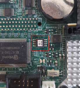
The circle marking the location of pin 1 is highlighted red in the above image. The circle is a subtle indentation on the chip that can be seen with the aid of a flashlight.. | The circle marking the location of pin 1 is highlighted red in the above image. The circle is a subtle indentation on the chip that can be seen with the aid of a flashlight.. | ||
== User Builds == | == User Builds == | ||
Revision as of 18:22, 3 May 2025
| H8QGi+-F | |
|---|---|
 | |
| Overview | |
| Manufacturer | SuperMicro |
| Specifications | |
| Socket | 4x G34 |
| Northbridge | AMD SR5690 |
| Southbridge | AMD SP5100 |
| Super I/O | Winbond W83527DHG-P |
| BMC | Nuvoton WPCM450 |
| BMC Flash Location | Onboard |
| Memory | 32 slots (4 channels) DDR3-1600 ECC RDIMM/UDIMM, up to 1024GB |
| BIOS Flash | 2 MiB soldered SOIC-8 (W25Q16V) |
| Form Factor | SWTX |
| Power Inputs | 2x 8-pin EPS |
| Expansion Slot |
|
| Onboard Peripherals | |
| Graphics Adapter | Matrox G200eW |
| Network Interface | 2x Intel 82576 Gigabit |
| Storage Controller | SP5100's SATA2 (3.0 Gbps) |
| USB Controller | SP5100's onboard USB 2.0 |
| Serial Interface | One external, one internal |
| Audio Interface | None |
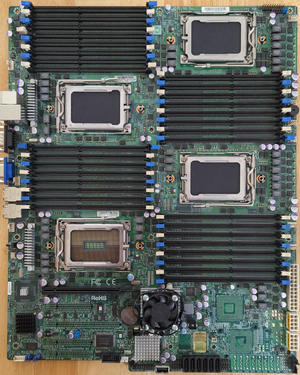
Several variants of the H8QGi motherboard are highly supported by coreboot-15h, namely the H8QGi+-F and H8QG6+-F. The H8QGi motherboards have 4 G34 sockets, each with 8 DIMM slots; supporting a maximum configuration of 64 cores and 1 TB of RAM. LRDIMM modules may bring the maximum memory up to 2 TB, but LRDIMM support has not been tested.
Board Variants
H8QGi+-F
The H8QGi+-F is the base model of the H8QGi series, all other variants have additional features. Compatibility of the onboard BMC with coreboot has not been tested; it can be disabled via the "JPB1" motherboard jumper.
H8QG6+-F
The H8QG6+-F has an onboard SAS controller; it can be flashed to IT mode.
H8QGi+-LN4F
The H8QGi+-LN4F has four onboard LAN ports. It is likely compatible with the coreboot image for H8QGi+-F, but this has not been tested.
H8QG7+-LN4F
The H8QG7+-LN4F has an onboard SAS controller and four onboard LAN ports. It is likely compatible with the coreboot image for H8QG6+-F, but this has not been tested.
H8QGi-F
The H8QGi-F is a H8QGi+-F with a secondary northbridge and additional PCIe lanes. The coreboot image for the H8QGi+-F can be used, but the secondary northbridge and associated PCIe lanes will be offline.
H8QG6-F
The H8QG6-F is a H8QG6+-F with a secondary northbridge and additional PCIe lanes. The coreboot image for the H8QG6+-F can be used, but the secondary northbridge and associated PCIe lanes will be offline.
H8QGi-LN4F
The H8QGi-LN4F is a H8QGi+-LN4F with a secondary northbridge and additional PCIe lanes. It is likely compatible with the coreboot image for H8QGi+-F, but this has not been tested; the secondary northbridge and associated PCIe lanes will be offline.
H8QG7-LN4F
The H8QG7-LN4F is a H8QG7+-LN4F with a secondary northbridge and additional PCIe lanes. It is likely compatible with the coreboot image for H8QG6+-F, but this has not been tested; the secondary northbridge and associated PCIe lanes will be offline.
Board Diagrams
Board Components
Socket G34

G34 was launched on March 29, 2010. It supports 10h and 15h Opteron CPU's[1]. All G34 Opteron CPUs are dual node processors with two NUMA nodes.
AMD Opteron 6100 Series
Processors in the AMD Opteron 6100 Series were designed with the K10 microarchitecture and are compatible with the G34 socket.
Official Source Code and Documentation
- AGESA Source Code
- AGESA Interface Specification
- BIOS and Kernel Developer's Guide
- Product Data Sheet
- Power and Thermal Data Sheet
AMD Opteron 6200 and 6300 Series
Processors in the AMD Opteron 6200 and 6300 Series were designed with the Bulldozer (6200 series) and Piledriver (6300 series) microarchitectures and are compatible with the G34 socket.
Official Source Code and Documentation
- AGESA Source Code
- AGESA Interface Specification
- BIOS and Kernel Developer's Guide
- Product Data Sheet
- Software Optimization Guide
AMD SR5690
The AMD SR5690, also known as RD890S, was released in March 2010 as a powerful system logic for server and workstation platforms. It offers 46 PCI Express lanes, with 42 lanes dedicated to external PCIe devices and 4 for the A-Link Express II interface to AMD's Southbridges like the SP5100 (formerly SB700S). The chipset boasts the latest technologies, including HyperTransport™ 3 and PCIe Gen 2, and its highly integrated, thermally efficient design comes in a compact 29mm x 29mm package.[2]
Official Source Code and Documentation
- CIMx Source Code
- BIOS Developer's Guide
- IOMMU Specification
- Register Reference Guide
- Register Programming Requirements
- Product Databook
- Product Errata
Part Numbers
- AMD 215-0716022
- AMD 215-0716038
- AMD 215-0716056
AMD SR5670
The AMD SR5670, formerly known as RD870S, is a versatile system logic designed for the latest server/workstation platform, supporting AMD's next-generation CPUs. The chipset features 34 PCI Express® (PCIe®) lanes, with 30 lanes dedicated to external PCIe devices and 4 for the A-Link Express II interface to AMD's Southbridges like the SP5100 (formerly SB700S). Utilizing HyperTransportTM 3 and PCIe Gen 2 technologies, the SR5670 offers high performance and reliability in a compact 29mm x 29mm package. [3]
Official Source Code and Documentation
- CIMx Source Code
- BIOS Developer's Guide
- IOMMU Specification
- Register Reference Guide
- Register Programming Requirements
- Product Databook
- Product Errata
AMD SP5100
The AMD SP5100 is a versatile Southbridge designed to complement AMD's server Northbridges, integrating essential I/O, communication, and other features for advanced server platforms into a single device. [4]
Official Source Code and Documentation
- CIMx Source Code
- BIOS Developer's Guide
- Register Reference Guide
- Register Programming Requirements
- Product Databook
- Product Errata
Part Numbers
- AMD 218-0660013
- AMD 218-0660024
- AMD 218-0660026
Nuvoton WPCM450
The Nuvoton WPCM450 is a combined Baseboard Management Controller and 2D/VGA-compatible Graphics Core with PCI Interface, Virtual Media, Keyboard and KVMR Module[5]. Multiple vendors shipped the WPCM450 with Linux, making it feasible to build an open source replacement for the original BMC firmware[6][7][8]. 3rd party documentation and tools have been developed by neuschaefer and are available on github. The WPCM450 appears to be related to, or based on, the Winbond W90N745.
Missing Features
- Support for the secondary SR5670 has not been implemented (PCIe slot 2 is offline).
- Support for the SR5690/SR5670 IOMMU has not been implemented.
Flashing Firmware
To switch from the stock firmware to coreboot, external flashing is required.
Flash Chip Location
The flash chip is located below the circular CMOS battery slot.
Flash Chip Orientation
The circle marking the location of pin 1 is highlighted red in the above image. The circle is a subtle indentation on the chip that can be seen with the aid of a flashlight..
User Builds
References
- ↑ https://en.wikipedia.org/wiki/Socket_G34
- ↑ https://theretroweb.com/chips/5696
- ↑ https://theretroweb.com/chips/5697
- ↑ https://theretroweb.com/chips/5699
- ↑ https://theretroweb.com/chips/10379
- ↑ https://github.com/neuschaefer/linux/tree/vendor/wpcm450-aten
- ↑ https://github.com/neuschaefer/linux/tree/vendor/wpcm450-ami
- ↑ https://github.com/neuschaefer/linux/tree/vendor/dell-idrac6-1.70
